
Build a Buck-Boost Converter
A buck-boost converter is a DC-DC power converter capable of producing an output voltage either higher or lower than its input. This makes it useful when the input voltage varies or when a regulated output must be maintained over a wide input-voltage range.
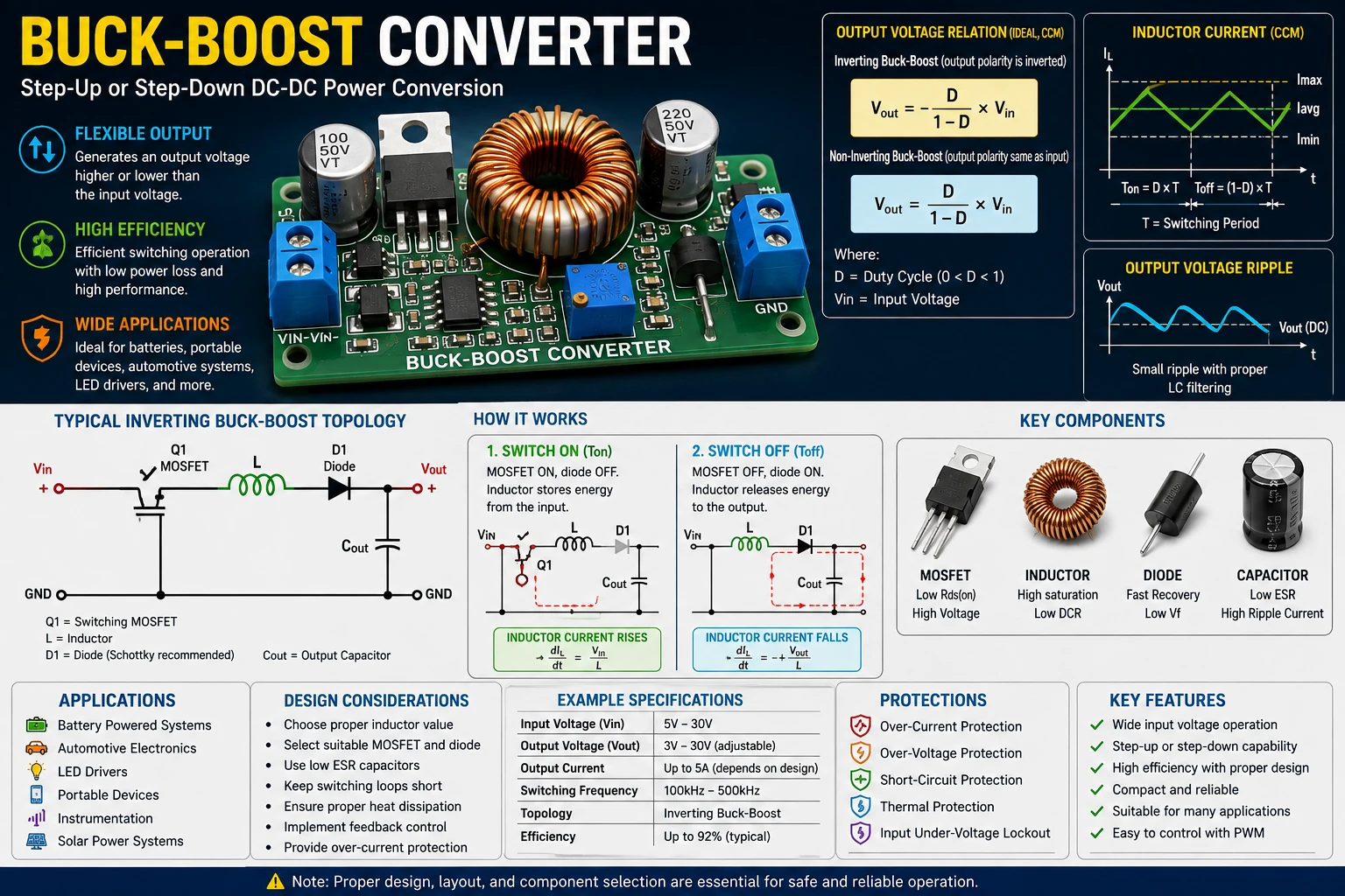
Project Overview
A buck converter can only reduce voltage, while a boost converter can only increase voltage. A buck-boost converter combines the ability to increase or decrease voltage in a single power-conversion stage.
DC Input
   │
   ▼
Switching Converter
   │
   ├── Inductor
   ├── MOSFET
   ├── Diode / Synchronous Switch
   └── Capacitor
   │
   ▼
Regulated DC Output
The control circuit continuously adjusts the switching duty cycle to maintain the desired output voltage.
Why Use a Buck-Boost Converter?
A buck-boost converter is useful when the input voltage can move both above and below the required output voltage.
For example, a battery may start at a voltage higher than the desired output and fall below it as it discharges.
- Battery-powered equipment.
- Portable electronics.
- Automotive electronics.
- LED power supplies.
- Instrumentation.
- Embedded systems.
- Solar-powered equipment.
Buck vs Boost vs Buck-Boost
| Converter | Output Relationship | Main Function |
|---|---|---|
| Buck | Lower than input | Step-down |
| Boost | Higher than input | Step-up |
| Buck-Boost | Higher or lower than input | Step-up / Step-down |
Basic Buck-Boost Operation
In the classical inverting buck-boost topology, the switching element controls the energy stored in the inductor.
              Switch
Input ────────┤
              │
              ▼
           Inductor
              │
              ├────► Diode ───► Output
              │
             GND
During one part of the switching cycle, energy is stored in the inductor.
During the other part, the stored energy is transferred to the output.
Important Buck-Boost Topologies
The term buck-boost can refer to several different converter arrangements.
- Classical inverting buck-boost.
- Non-inverting buck-boost.
- SEPIC converter.
- Zeta converter.
- Four-switch buck-boost converter.
The topology should be selected according to the required output polarity, efficiency, current range and control requirements.
Inverting Buck-Boost
The classical buck-boost converter produces an output with polarity opposite to the input.
In the ideal continuous-conduction case, the magnitude of the voltage relationship is approximately:
Vout = -Vin × D / (1-D)
where D is the switching duty cycle.
The negative sign indicates the reversed output polarity.
Duty Cycle
The duty cycle is the fraction of each switching period during which the main switching device is conducting.
D = Ton / T
Increasing the duty cycle changes how much energy is transferred through the converter.
The exact relationship depends on the topology and operating mode.
Example
Consider an ideal inverting buck-boost converter with:
Vin = 12 V
D = 0.5
The ideal output magnitude is:
|Vout| = 12 × 0.5 / (1 - 0.5)

|Vout| = 12 V
The output polarity is opposite to the input in the classical topology.
Inductor
The inductor is one of the most important components in the converter.
It stores energy during one part of the switching cycle and releases that energy during another part.
The inductor must be selected according to:
- Inductance.
- Peak current.
- RMS current.
- Saturation current.
- DC resistance.
- Core losses.
- Switching frequency.
Inductor Energy
The energy stored in an inductor is:
E = ½ × L × I²
As the current increases, stored energy increases with the square of the current.
This makes saturation and thermal limits particularly important at high output power.
Inductor Ripple Current
The switching operation causes the inductor current to rise and fall.
Current

  /\/\/\/\/\/\/\
 /              \
/                \

──────────────────── Time
The difference between the maximum and minimum current is the inductor ripple current.
The selected ripple level affects the inductor size, semiconductor current stress and output ripple.
MOSFET Switching Device
A MOSFET is commonly used as the main switching element.
It rapidly alternates between conducting and non-conducting states.
Important MOSFET parameters include:
- Drain-source voltage rating.
- Drain current rating.
- RDS(on).
- Gate charge.
- Switching speed.
- Thermal resistance.
Adequate voltage and current margins should be provided.
Diode
In an asynchronous converter, a diode provides the path for inductor current during the appropriate switching interval.
The diode must be selected according to:
- Reverse voltage.
- Forward current.
- Forward voltage.
- Switching speed.
- Thermal dissipation.
At higher switching frequencies, diode recovery characteristics can become important.
Synchronous Buck-Boost
A synchronous design replaces one or more diodes with controlled MOSFETs.
This can reduce conduction losses, particularly at low output voltages and high currents.
The control system becomes more complicated because the switching devices must be timed correctly.
Output Capacitor
The output capacitor smooths the pulsed current delivered by the converter.
The capacitor must have suitable:
- Voltage rating.
- Capacitance.
- Ripple-current rating.
- ESR.
- Temperature rating.
Low-ESR capacitors can reduce output ripple, although the complete control loop must be designed around the actual capacitor characteristics.
PWM Controller
A PWM controller regulates the converter by adjusting the switching duty cycle.
Reference Voltage
       │
       ▼
Error Amplifier
       │
       ▼
PWM Controller
       │
       ▼
Gate Driver
       │
       ▼
MOSFET
       │
       ▼
Power Stage
       │
       ▼
Output
       │
       └──── Feedback
The controller continuously responds to changes in input voltage and load.
Voltage Feedback
The output voltage is normally reduced to a suitable feedback level using a resistor divider.
Vout
 │
 R1
 │
 ├────► Feedback
 │
 R2
 │
GND
The controller compares the feedback voltage with an internal or external reference.
The duty cycle is then adjusted to maintain regulation.
Current Sensing
Current sensing allows the controller to detect excessive current and can also be used for current-mode control.
Switch Current
      │
      ▼
Sense Resistor
      │
      ▼
Current Sense
      │
      ▼
Controller


The sense resistor produces a small voltage proportional to current.

  Vsense = I × Rsense
Continuous and Discontinuous Conduction
Buck-boost converters can operate in continuous conduction mode (CCM) or discontinuous conduction mode (DCM).
In CCM, the inductor current does not fall to zero during a switching cycle.
In DCM, the inductor current falls to zero before the next switching cycle begins.
The converter equations, control behavior and component stresses differ between the two modes.
Switching Frequency
Higher switching frequency can reduce the required inductance and capacitance.
However, switching losses and electromagnetic interference generally increase as frequency increases.
The operating frequency should therefore be selected as a compromise between component size, efficiency, thermal performance and EMI.
Efficiency
Converter efficiency is calculated as:
Efficiency = Output Power / Input Power × 100%
Losses occur in the MOSFET, diode, inductor, capacitors, PCB traces and other components.
At high current, even a small resistance can result in significant power loss.
Thermal Management
Power semiconductor losses become heat.
At higher power levels, heatsinks or forced-air cooling may be required.
The temperature of the MOSFET, diode and inductor should remain within their rated operating limits.
Input and Output Voltage Range
One of the main advantages of the buck-boost topology is its ability to operate when the input voltage moves through the desired output voltage.
For example, a battery whose voltage changes from above the required output to below it can still be regulated using a suitable non-inverting buck-boost architecture.
Non-Inverting Buck-Boost
A non-inverting buck-boost converter maintains the same output polarity as the input.
A four-switch arrangement is one practical implementation.
VIN │ ┌───┴───┐ │ │ MOSFET MOSFET │ │ ├───┬───┤ │ Inductor │ ┌───┴───┐ │ │ MOSFET MOSFET │ │ └───┬───┘ │ GND │ VOUT
The controller can operate the power stage as a buck converter when the input is above the desired output and as a boost converter when the input is below it.
SEPIC Converter
A SEPIC converter is another non-inverting topology capable of producing an output voltage above or below the input.
It uses coupled energy-storage paths and a series capacitor.
SEPIC converters can be useful when input polarity must be preserved.
Input Protection
- Input fuse.
- Reverse-polarity protection.
- Input transient suppression where appropriate.
- Input filtering.
- Over-current protection.
Over-Voltage Protection
A feedback failure can potentially cause the output voltage to rise above its intended value.
An independent over-voltage protection mechanism can disable the converter if an unsafe condition is detected.
Short-Circuit Protection
A shorted output can cause the converter to attempt to deliver excessive current.
Current limiting should prevent the power components from being subjected to destructive stress.
Depending on the controller, protection may use cycle-by-cycle current limiting, shutdown or hiccup-mode operation.
Soft Start
A soft-start function gradually increases the converter's duty cycle or current limit during startup.
This reduces startup stress on the inductor, MOSFET, input source and output capacitor.
PCB Layout
Switching converters are sensitive to PCB layout.
- Keep high-current switching loops short.
- Place input capacitors close to the switching stage.
- Keep gate-drive traces short.
- Separate feedback wiring from noisy switching nodes.
- Use adequate copper width.
- Provide appropriate thermal paths.
- Minimize parasitic inductance.
Testing the Converter
Testing should begin with a current-limited source and a low load.
- Inspect the PCB.
- Check component orientation.
- Verify the MOSFET and diode.
- Check the inductor.
- Verify the controller supply.
- Check the switching frequency.
- Check the gate-drive waveform.
- Apply a low input voltage where practical.
- Start with a small load.
- Increase the load gradually.
- Monitor output voltage and temperature.
- Measure efficiency at several operating points.
Oscilloscope Measurements
Useful waveforms include:
- MOSFET gate voltage.
- Switching-node voltage.
- Inductor current.
- Current-sense signal.
- Output ripple.
- Feedback voltage.
The measurement equipment must be connected appropriately for the voltage levels and topology being tested.
Troubleshooting
No Output Voltage
- Check the input voltage.
- Check the controller supply.
- Check the switching signal.
- Check the MOSFET.
- Check the diode or synchronous switch.
- Check the inductor.
- Check the feedback circuit.
Output Voltage Too High
- Check the feedback divider.
- Check the reference voltage.
- Check feedback polarity.
- Check the controller.
- Check for an open feedback connection.
Output Voltage Too Low
- Check input voltage.
- Check duty cycle.
- Check inductor saturation.
- Check MOSFET losses.
- Check diode losses.
- Check excessive load current.
MOSFET Gets Hot
- Check switching losses.
- Check gate-drive voltage.
- Check switching frequency.
- Check RDS(on).
- Check heatsinking.
- Check for excessive current.
Output Has Excessive Ripple
- Check output capacitor.
- Check capacitor ESR.
- Check inductor ripple current.
- Check switching frequency.
- Check PCB layout.
Common Mistakes
- Choosing an inductor with insufficient saturation current.
- Using an undersized MOSFET.
- Ignoring diode losses.
- Using inadequate output capacitance.
- Poor PCB layout.
- Insufficient current protection.
- Incorrect feedback polarity.
- Testing immediately at maximum power.
Safety Notes
- Use a current-limited power source during initial testing.
- Do not exceed the voltage ratings of any component.
- Provide appropriate fusing.
- High-current batteries can produce dangerous short-circuit currents.
- Use suitable heatsinks where required.
- Do not work on energized high-voltage circuits.
- Use appropriately rated measurement equipment.
Skills Learned
- Buck-boost converter operation.
- PWM control.
- Inductor energy storage.
- MOSFET switching.
- Current sensing.
- Voltage feedback.
- Power semiconductor selection.
- Thermal management.
- DC-DC converter testing.
- Switching power-supply troubleshooting.
Key Points
- A buck-boost converter can increase or decrease the input voltage.
- The inductor stores and transfers energy during each switching cycle.
- PWM controls the amount of energy transferred.
- The classical buck-boost topology produces inverted output polarity.
- Non-inverting buck-boost topologies preserve output polarity.
- Feedback maintains a regulated output voltage.
- Current sensing provides protection and can support current-mode control.
- Inductor saturation must be avoided.
- PCB layout strongly affects switching performance.
- Thermal management becomes increasingly important as output power increases.